Sub-Micron Surface Roughness Impact on Sub-Terahertz Waveguide Transmission Loss in Metallized Injection Tooling
Sub-micron cavity surface finish controls sub-terahertz waveguide loss; lowering roughness below skin depth halves attenuation in metallized injection parts.


Skin
Conductor boundary physics above 100 gigahertz dictates signal attenuation. At sub-terahertz frequencies, electromagnetic fields penetrate metals only to a shallow depth, concentrating current along the innermost boundary layer. Skin depth contracts as operating frequency rises, focusing ohmic losses within the top few nanometers of the plating layer.

Electromagnetic Current Confinement at Sub-Terahertz Frequencies
High-frequency signals propagate through an extremely thin region along the inner surface of a metallic channel. Skin depth depends on bulk electrical resistivity, magnetic permeability, and frequency. In pure copper, skin depth is roughly 206 nanometers at 100 gigahertz, falling to 139 nanometers at 220 gigahertz and 119 nanometers at 300 gigahertz.
These dimensions set the allowable limits for cavity surface finish.
Surface roughness forces current off a straight path. When peak-and-valley irregularities exceed skin depth, current follows the physical contours of the surface, lengthening the effective conduction path and pushing surface resistance above smooth-wall theoretical models.

Conductor Depth Mechanics in Micro-Rough Conductors
In the sub-terahertz range, current density drops exponentially beneath the conductor surface. Tooling marks, peaks, and valleys disrupt uniform current distribution, concentrating charge at surface transitions and driving up both thermal dissipation and signal attenuation.
| Frequency Band | Center Frequency (GHz) | Copper Skin Depth (nm) | Silver Skin Depth (nm) | Critical Roughness Rq Limit (nm) |
|---|---|---|---|---|
| W-Band | 95 | 212.1 | 204.3 | 106.0 |
| D-Band | 140 | 174.2 | 167.8 | 87.1 |
| G-Band | 220 | 138.9 | 133.8 | 69.4 |
| H-Band | 300 | 118.9 | 114.5 | 59.4 |
Silver has a lower bulk resistivity than copper, yielding a skin depth of 133.8 nanometers at 220 gigahertz. However, once surface features approach critical roughness thresholds, profile irregularities dominate attenuation in both metals, overriding any advantage in base conductivity.
Failing to control sub-micron cavity roughness drives up waveguide attenuation, forcing higher RF output power that quickly exhausts system power budgets.


Finish
Producing mirror-quality mold inserts requires dedicated diamond machining and optical polishing. Cavity polishability depends heavily on tool steel selection; standard alloys contain carbide inclusions that tear out during abrasive polishing, leaving micro-voids behind. Sub-terahertz waveguide inserts rely instead on electroless nickel-phosphorus, beryllium-copper alloys, or vacuum-melt stainless steels to maintain smooth, inclusion-free cavity surfaces.

Ultra-Precision Tool Machining and Diamond Turning Mechanics
Single-crystal diamond cutting tools produce mirror surfaces on non-ferrous cavity inserts, achieving root-mean-square roughness values below 5 nanometers without traditional machining marks. Spindle stability and feed dynamics dictate the resulting spatial frequencies, preventing periodic tool chatter that would otherwise scatter RF energy in sub-terahertz channels.
Machining ferrous tool steels directly demands ultrasonic-assisted diamond tooling or high-speed milling followed by manual optical polishing. Manual polishing, however, introduces spatial variability across cavity corners and rounds critical rectangular waveguide edges. Diamond-turning single-point profiles into electroless nickel-plated steel avoids edge rounding and produces deterministic cavity geometry.
Roughness elevates conductor power dissipation when localized peak-to-valley heights exceed fifty percent of the electromagnetic skin depth.
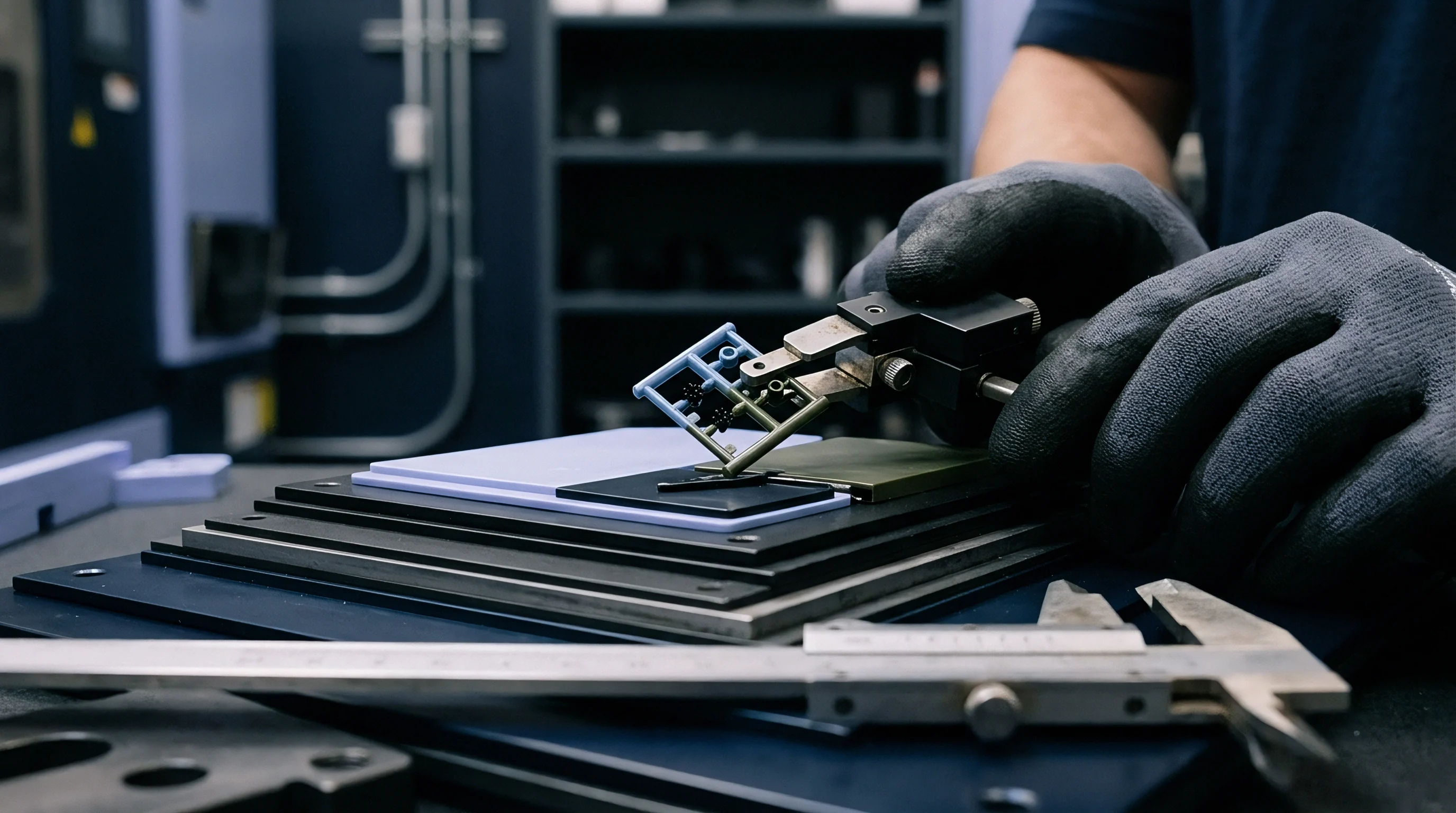
Steel Cavity Micro-Topography Measurement Standardisation
Optical white-light interferometers measure three-dimensional surface profiles without touching delicate cavity walls. Characterizing these surfaces requires assessing arithmetic average roughness, root-mean-square roughness, and developed interfacial area ratio, using spatial frequency metrics to separate short-wavelength roughness from mid-spatial waviness.
- Mount cavity insert onto an isolated optical table with vibration dampening controls.
- Calibrate white-light interferometer using certified optical step height calibration blocks under ISO 25178 standards.
- Scan five localized evaluation zones within the internal waveguide channel floor and side walls using a 50x optical magnification lens.
- Apply a high-pass spatial filter at 0.08 millimeter cutoff length to isolate micro-roughness from macro-geometric channel form errors.
- Extract root-mean-square spatial surface parameters and verify surface slope distribution across the waveguide profile.
Unexpected micro-ridge patterns on electroplated nickel inserts often trace to spindle vibration during final diamond turning passes.


Melt
Molding polymers at sub-micron scales requires precise thermal control at the tool interface. Filling intricate sub-terahertz cavity details demands high injection speeds and elevated mold temperatures to keep the resin fluid long enough to wet out micro-features before freezing occurs.

What Dictates Surface Replication Accuracy at Sub-Micron Scales?
High mold temperatures and rapid injection drive viscous polymers into fine cavity details. Conventional injection tooling chills molten polymer immediately upon contact with cold steel, creating a skin layer that fails to mirror the mold surface. Sub-terahertz molding relies on variothermal tooling to keep cavity surfaces above the polymer’s glass transition temperature throughout injection.
Sustaining steel temperatures above glass transition under high cavity pressure allows polymer chains to deform around nanometer-scale cavity features. Lowering mold temperatures below heat deflection before ejection locks in geometry without thermal distortion. Cyclic Olefin Polymers combine low dielectric loss with high replication fidelity, making them well suited for sub-terahertz substrates.
Incorporating variothermal mold temperature cycling above polymer glass transition temperature prevents premature skin freezing and ensures sub-micron surface feature replication.

Variothermal Tooling Dynamics and Viscous Shear Frozen Layers
Variothermal systems maintain boundary temperatures above glass transition using induction heating or pressurized hot-water channels placed directly behind cavity walls. These thermal responses must occur within seconds to maintain viable cycle times.
- Hesitation flow marks occur when melt fronts stall in thin waveguide ribs, causing step changes in local surface roughness.
- Jetting lines form during high-velocity injection through unrestricted gates, introducing linear defects that scatter propagating waves.
- Micro-sink depressions develop behind internal rib transitions, creating localized phase distortion inside waveguide channels.
- Shear-induced skin delamination occurs when extreme shear breaks polymer chains along the mold boundary during rapid packing.
If melt temperature drops below the processing window during micro-injection, surface replication degrades before pressure transfer finishes.


Plating
Metallization applies a conductive skin over the injection-molded polymer substrate using sputtering, vacuum deposition, or electroless plating. These metal layers must maintain uniform thickness around narrow waveguide corners and adhere strongly enough to withstand thermal cycling without peeling.

Electroless and Sputtered Layer Metallization Stacks
Physical vapor deposition applies a titanium or chromium seed layer measuring 20 to 50 nanometers, establishing a strong chemical bond with the polymer substrate without adding meaningful ohmic resistance. Sputtering yields highly uniform thin films across these plastic surfaces.
Electroless copper plating builds the primary conductive layer over the seed film. Unlike line-of-sight vapor deposition, electroless plating covers complex three-dimensional internal channels uniformly. Applying 1.5 to 3.0 micrometers of copper provides coverage exceeding ten skin depths at 220 gigahertz.
| Layer Function | Material Selection | Deposition Method | Target Thickness (nm) | Adhesion / Roughness Impact |
|---|---|---|---|---|
| Adhesion Layer | Titanium / Chromium | RF Magnetron Sputtering | 30 | Conforms to substrate topography without smoothing. |
| Primary Conductor | High-Purity Copper | Electroless Plating | 2000 | Bulks conductor thickness; risks nodular growth if un-controlled. |
| Diffusion Barrier | Nickel / Palladium | Electroless Plating | 100 | Prevents copper oxidation; slightly elevates ohmic loss. |
| Passivation Layer | Immersion Gold | Chemical Immersion | 50 | Protects underlying stacks; maintains long-term surface conductivity. |
Internal stresses developed as metal deposits thicken over micro-textured plastic can degrade surface finish and cause mechanical delamination.
Deposition Internal Stress and Interface Degradation
High tensile stress within electroless copper deposits can warp thin resin walls and distort internal channel cross sections. Regulating bath chemistry, pH, and plating temperature controls internal stress, preserving channel geometry and surface smoothness.
Electroless copper deposit stress exceeding fifty megapascals induces localized micro-wrinkling across flexible polymer waveguide walls.
- Verify substrate surface pre-treatment specifications to confirm chromic-acid-free etching parameters prior to seed layer sputtering.
- Check sputtering target purity levels to ensure metallic films maintain under ten parts per million oxygen contamination.
- Audit plating bath stress control additives using flexible strip contractometer tests every twenty-four operating hours.
- Inspect corner plating build-up ratio using destructive cross-sectional scanning electron microscopy on production validation parts.
Incorporating an explicit coating stress limit under ISO 14577 into supply contracts obligates platers to measure and document internal stress for every production lot.


Attenuation
Signal loss in sub-terahertz waveguides stems from bulk dielectric dissipation and surface resistance, with ohmic conduction losses dominating in metallized plastic structures. Rough cavity walls force currents over elongated surface contours, raising effective surface resistance above smooth-wall predictions.

Hammerstad and Gradient Attenuation Modeling in Sub-Micron Regimes
Predictive loss formulations adjust classical smooth-wall equations using surface topology metrics. The Hammerstad-Bekkadal model applies a correction factor based on root-mean-square roughness relative to skin depth, offering accurate predictions up to moderate roughness ratios.
When surface roughness approaches or exceeds skin depth, gradient attenuation models give more reliable loss estimates by representing micro-rough surfaces as stratified conductive layers that account for localized field scattering.
Applying gradient attenuation modeling reveals that surface roughness root-mean-square values equal to skin depth increase wave attenuation by ninety-four percent over theoretical smooth conductors.

Worked Construction of Attenuation Overhead across Cavity Roughness Tolerances
Evaluating a 220 gigahertz rectangular waveguide channel shows how cavity finish governs transmission efficiency. For a WR-4.3 waveguide with internal dimensions of 1.092 millimeters by 0.546 millimeters, operating at 220 gigahertz yields a copper skin depth of 139 nanometers. Theoretical attenuation for perfectly smooth copper walls at this frequency is roughly 0.12 decibels per centimeter.
A tool cavity finished by standard high-speed milling yields a polymer surface roughness of 250 nanometers root-mean-square, creating a roughness-to-skin-depth ratio of 1.80. The modified Morgan model calculates an attenuation factor of 2.15, increasing transmission loss to 0.258 decibels per centimeter. Over a 100 millimeter run, total loss reaches 2.58 decibels.
Refining cavity finish through ultra-precision diamond turning reduces polymer surface roughness to 20 nanometers root-mean-square, dropping the roughness ratio to 0.144. This lowers the attenuation correction factor to 1.02, yielding operational losses of 0.122 decibels per centimeter. Total attenuation over 100 millimeters falls to 1.22 decibels ~ saving 1.36 decibels of RF power and cutting signal loss roughly in half.
| Tool Finish Tier | Tool Machining Process | Polymer Surface Rq (nm) | Attenuation Factor (w_rough) | Transmission Loss (dB/cm) |
|---|---|---|---|---|
| Standard Polish (SPI B-1) | Manual Papering | 350 | 2.85 | 0.342 |
| Fine Polish (SPI A-2) | Diamond Paste Abrasive | 120 | 1.68 | 0.202 |
| Mirror Polish (SPI A-1) | Optical Lap Finishing | 45 | 1.12 | 0.134 |
| Ultra-Precision (Optical) | Single-Point Diamond Turning | 12 | 1.01 | 0.121 |
Whether molecular smoothing coatings applied over sputtered metal layers can compensate for mid-spatial cavity tool marks without degrading dielectric performance remains an open question in high-frequency manufacturing.
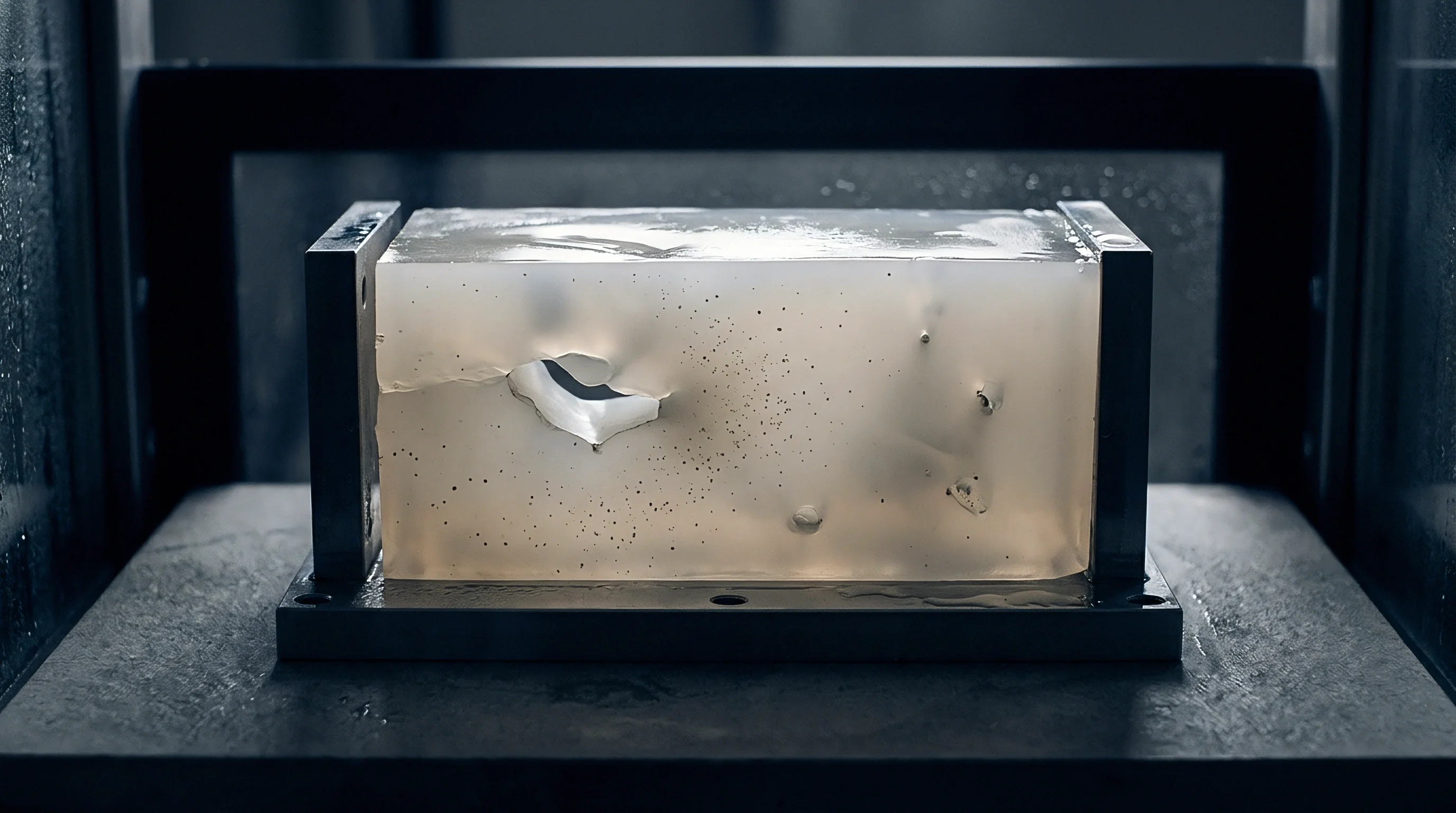

Contract
Procurement agreements for sub-terahertz components require explicit surface topology parameters. Standard tooling quotes relying on SPI polish callouts fail to constrain high-frequency performance. Incorporating three-dimensional surface roughness metrics under ISO 25178 into contracts protects against signal transmission failures in early tool samples.

Cavitation Amortisation and Surface Degradation Life Cycles
Amortizing tool costs across high-volume production requires monitoring cavity surface wear. High-velocity polymer flow carrying glass fillers or abrasive colorants degrades cavity micro-finishes over time. Continuous flow can erode a diamond-turned surface from 15 nanometers roughness to over 100 nanometers in fifty thousand shots, degrading signal propagation in molded parts.
Tooling supply contracts need explicit schedules for replacing nickel-phosphorus inserts or re-diamond-turning cavity surfaces. Budgeting for insert replacement or re-machining every thirty thousand shots maintains surface standards throughout long production runs.
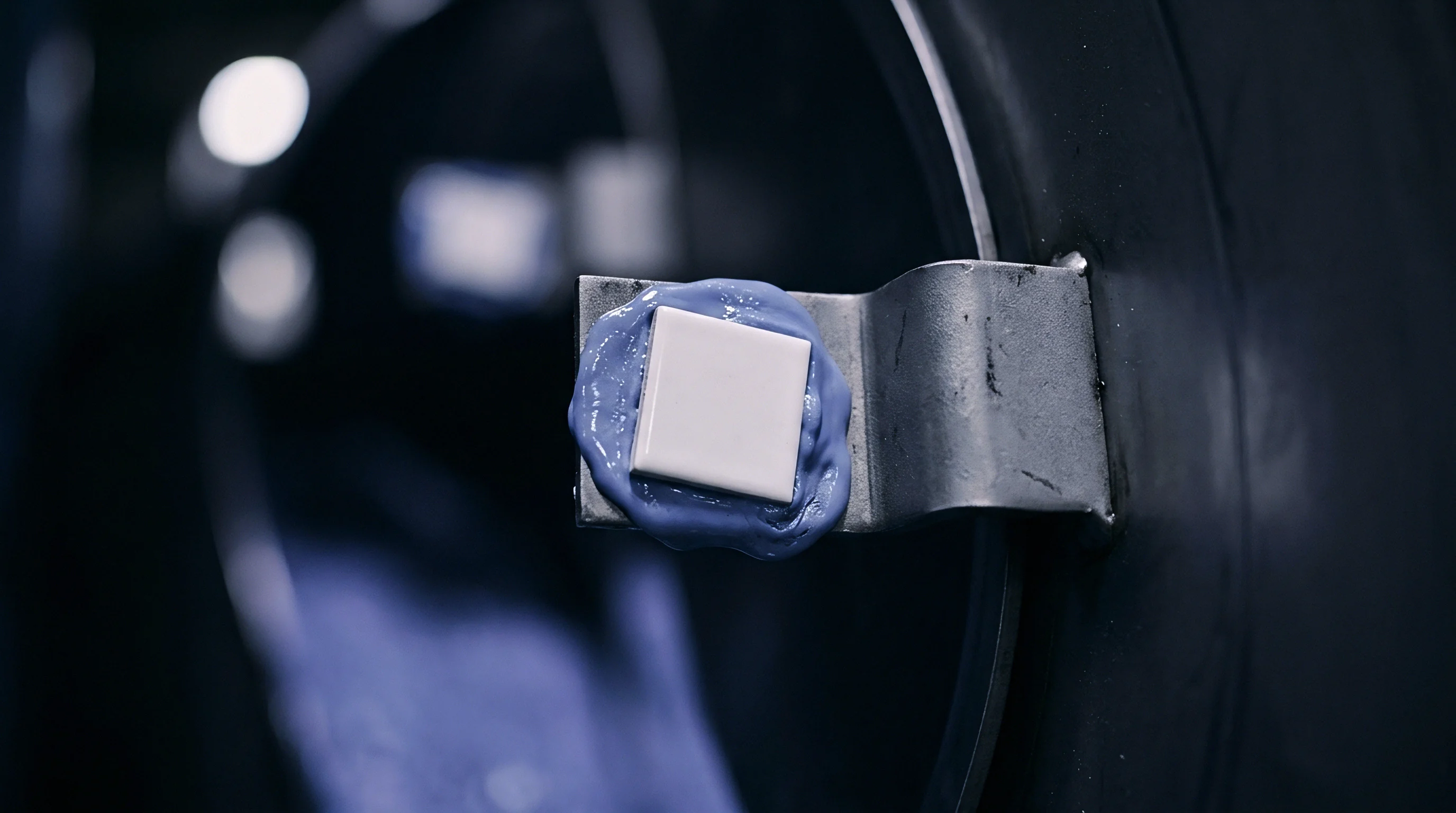
Sourcing Procurement Risk Allocation for Sub-Terahertz Waveguide Tooling
Enforceable contracts must separate macro dimensional tolerances from surface finish metrics. Dimensional tolerances under DIN 16742 ensure cut-off frequency compliance, while surface roughness controls attenuation limits. Requiring non-contact optical profilometry inspection reports for both raw cavity inserts and first-article metallized parts isolates defects and avoids scrap disputes between molders and plating subcontractors.
Auditing cavity surface quality before metallization separates tool finishing defects from downstream plating issues.