Electroformed Copper Mould Inserts Manufacturing Process Tolerances
Electroformed copper mould inserts achieve sub-micron surface reproduction but require low-stress sulfamate baths to limit dimensional distortion below 5 microns.
Mandrel
Master pattern preparation determines the foundational geometric envelope for electroformed copper tooling inserts. The physical substrate, known in electroforming as the mandrel, establishes every spatial dimension, draft angle, and surface micro-structure that the deposited copper layer subsequently envelopes. Variations in the mandrel’s dimensional stability, thermal expansion during plating, or surface conductivity translate into geometric error within the finished insert shell.
Sub-Micron Patterning and Lithographic Masters
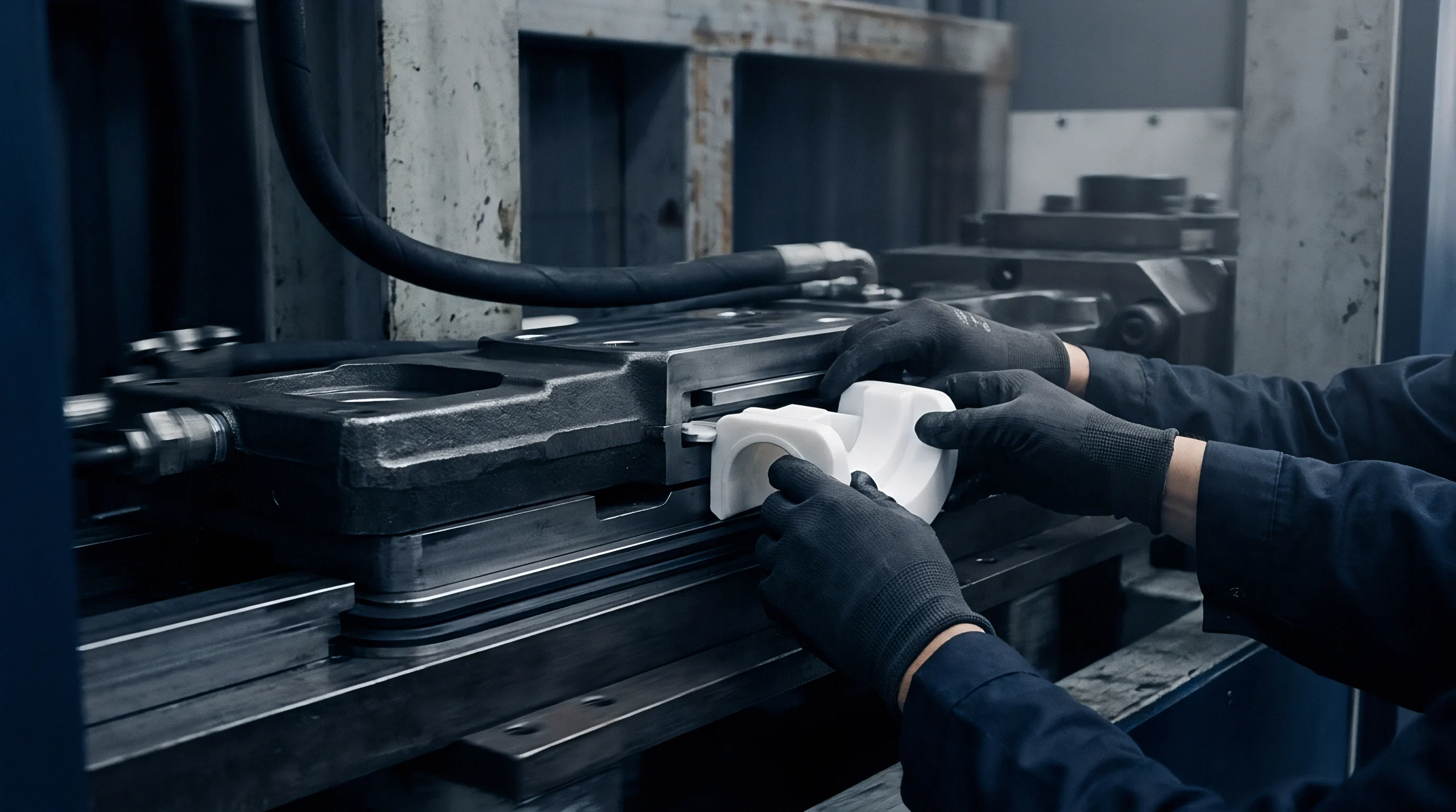
Silicon and optical-grade glass substrates serve as the primary mandrels when manufacturing micro-structured or optical-grade mold inserts. Photoresist coating, combined with direct-write electron beam lithography or photolithography, yields sub-micron feature definitions with edge roughness held below 5 nanometers. Glass and silicon exhibit low thermal expansion coefficients (0.55 × 10⁻⁶ /K for fused silica and 2.6 × 10⁻⁶ /K for silicon), suppressing dimensional drift when exposed to acid plating bath temperatures ranging from 30°C to 50°C. Metallic seed layers of chromium-gold or nickel-chromium applied via physical vapor deposition establish electrical conductivity across non-conductive lithographic surfaces without filling critical micro-textures.
Copper plating deposits slowly. The deposition proceeds atom by atom, causing the copper layer to replicate substrate details down to 10 nanometers. Sub-micron features mirror the master.
If the photoresist sidewall exhibits a 2-degree taper error from uncalibrated UV light exposure, that angular error reproduces across every electroformed insert generated from that master.
- Lithographic Photoresist Exposure establishes micro-textured geometry on silicon or glass substrates, where a sub-micron defocusing error alters side-wall draft angles and compromises part release.
- Conductive Metallization Coating places a nanoscale silver or nickel seed layer over non-conducting surfaces, creating uniform cathode potential to prevent localized plating thickness spikes.
- Passivation Layer Application generates a controlled oxide or dichromate film, balancing clean release forces against premature delamination during early metal deposition.
- Precision Mounting and Mandrel Masking seals non-functional areas with chemical-resistant stop-off lacquer, directing current distribution exclusively to active cavity surfaces.
Machined Metal Substrates and Surface Passivation
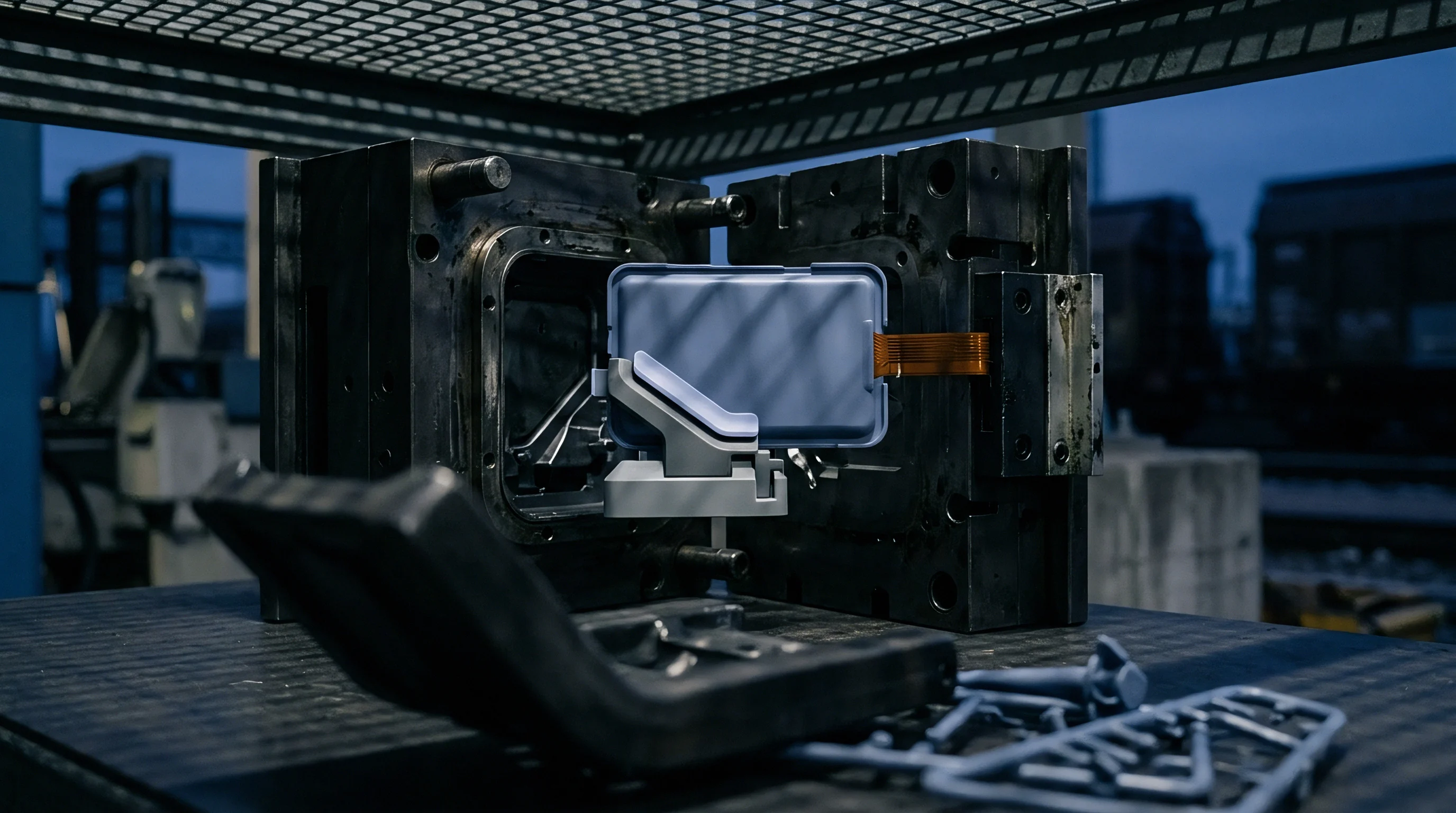
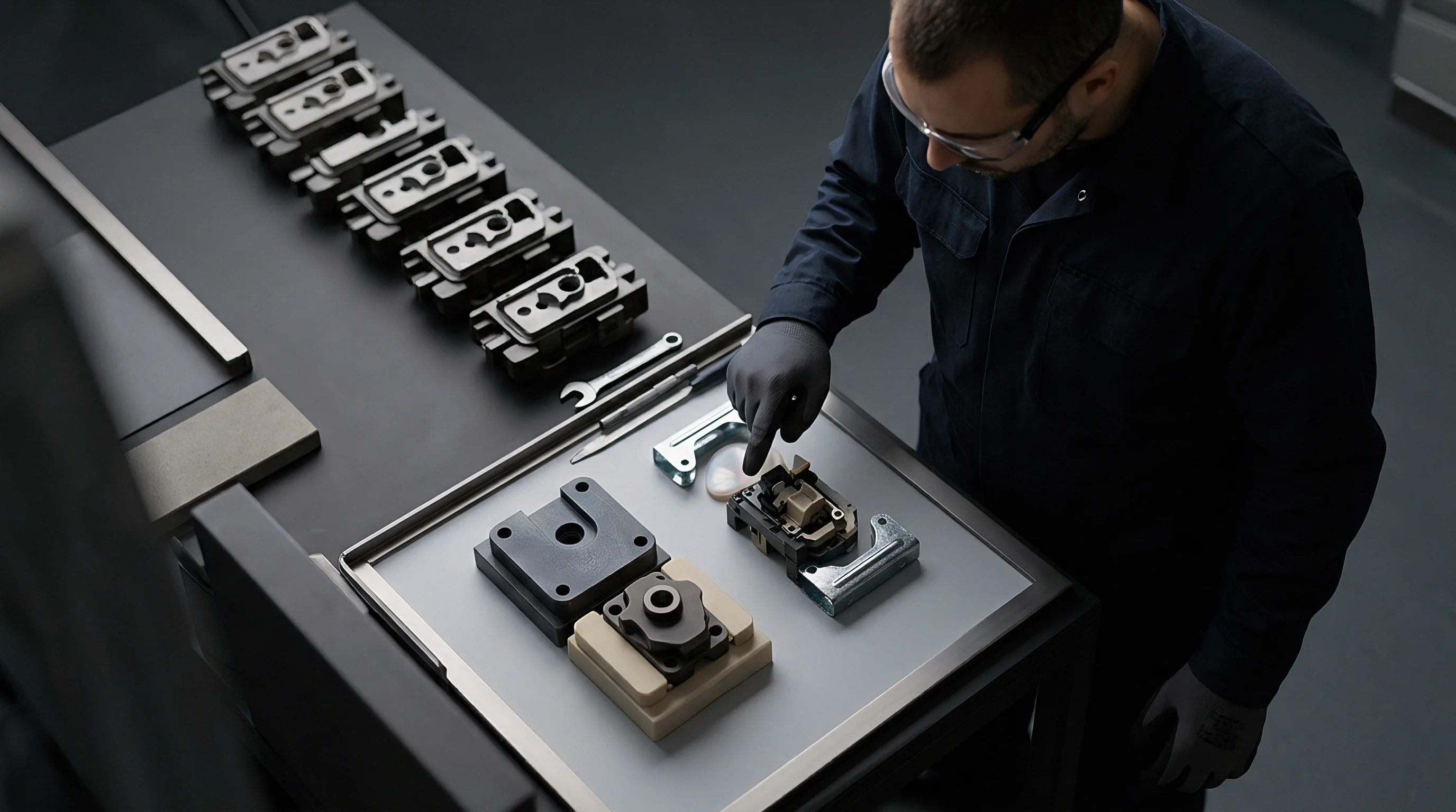
Directly machined metal mandrels handle larger macro-scale cavity geometries containing complex three-dimensional contours. Stainless steel grades AISI 303 and AISI 316, along with free-cutting brass (UNS C36000), act as reusable mandrels after receiving surface passivation treatments. Passivation films dictate separation success.
Substrates constructed from stainless steel form self-passivating chromium oxide layers under nitric acid treatment (20% to 30% HNO₃ volume fraction at 50°C for 30 minutes). This oxide layer acts as an electron-permeable insulating barrier, preventing chemical atomic bonding between the plating bath metal and the base substrate while permitting metallic deposition.
Machined brass mandrels demand chemically applied separation coatings, such as nickel dichromate conversion films or monomolecular chemical release agents. Excessive passivation thickness increases contact resistance, causing non-uniform cathode potential that shifts initial deposition rates across the mandrel face. Insufficient passivation results in mechanical locking, forcing toolmakers to dissolve the mandrel in nitric acid or alkaline stripping baths, which risks etching the internal cavity walls of the copper insert.
Toolmakers often explain away cavity oversize discrepancies by citing unaccounted thermal growth of brass mandrels operating within warm electroforming electrolytes.
Electrodeposition
Bath chemistry and current distribution dictate the crystal growth mechanics of the growing metal shell. Electroforming relies on the controlled reduction of cupric ions onto the mandrel cathode surface. Internal stress development within the deposited copper matrix acts as the primary driver of macro-scale distortion, shell twisting, and pitch-line pitch errors once the deposit detaches from the master substrate.
Sulfamate versus Sulfate Electrolyte Formulations
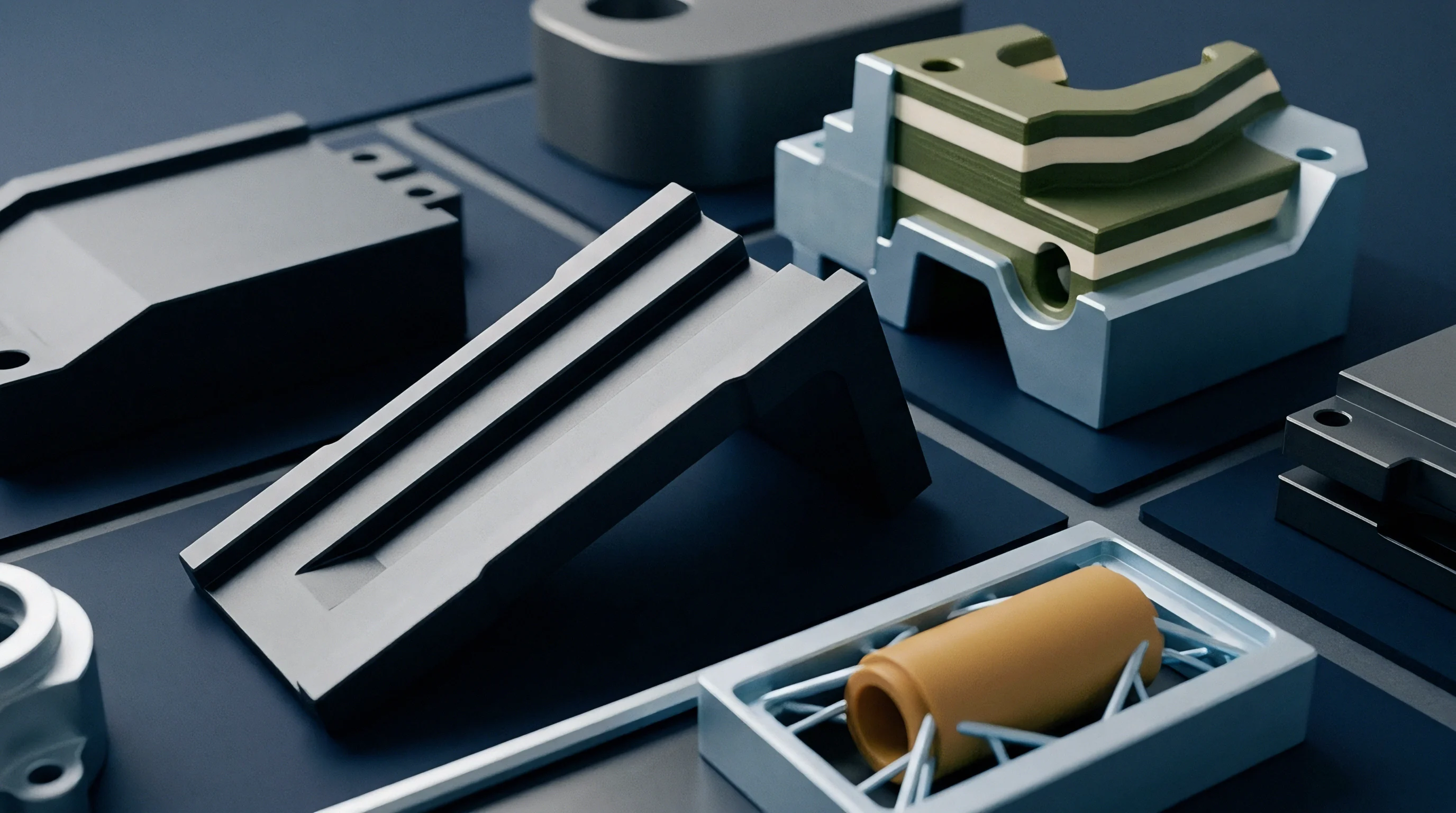
Copper sulfamate baths and acid copper sulfate baths represent the two dominant chemistry families for electroforming mold inserts. Acid copper sulfate solutions (containing 180 to 220 g/L CuSO₄·5H₂O and 50 to 70 g/L H₂SO₄) offer high bath stability and low operating costs, operating at current densities between 2 and 5 A/dm². Acid sulfate deposits yield tensile stress levels between 15 MPa and 35 MPa, which induces inward bowing on deep-cavity shell geometries.
Copper sulfamate chemistry (utilizing Cu(NH₂SO₃)₂ operated with organic stress reducers such as naphthalene-1,3,6-trisulfonic acid) reduces internal stress down to a range of -5 MPa compressive to +5 MPa tensile.
Internal stress distorts geometry. Compressive stress causes the electroformed shell to flare outward upon mandrel release, while tensile stress causes internal collapse across long unsupported spans. Maintaining electrolyte purity requires continuous active carbon filtration to capture organic breakdown products that alter grain orientation and increase internal lattice strain.
Low current density combined with active bath agitation minimizes internal tensile stress during shell growth.
| Electrolyte Type | Current Density (A/dm²) | Operating Temp (°C) | Internal Stress (MPa) | Vickers Hardness (HV 0.1) |
|---|---|---|---|---|
| Acid Copper Sulfate | 2.0 – 5.0 | 25 – 35 | +15 to +35 (Tensile) | 80 – 120 |
| Copper Sulfamate | 1.5 – 4.0 | 40 – 50 | -5 to +5 (Neutral) | 140 – 220 |
| Hard Copper (Additive-Assisted) | 1.0 – 3.0 | 30 – 40 | +5 to +15 (Tensile) | 220 – 280 |
Current Density and Internal Stress Control
Electric field lines concentrate around sharp convex corners on the cathode mandrel, creating localized current density spikes. High local current density drives rapid grain growth, producing coarse columnar microstructures with poor mechanical strength and uneven wall thickness. Recessed concave corners suffer from electric field shielding, yielding thin copper deposits that fail under molding pressure.
Shields, thieves, and conformal anodes homogenize current distribution across complex tool geometries. Non-conductive polypropylene shields block field lines traveling toward external corners, while auxiliary copper wire cathodes (thieves) burn off excess current density near high-profile edges. Current density controls crystal growth.
Maintaining precise cathode current densities within 0.2 A/dm² across the entire surface profile ensures uniform grain structure, maintaining tensile yield strength above 300 MPa across both thick and thin wall sections.
- Corner Thinning Defect occurs when high aspect ratio features shield electric field lines, reducing local deposit thickness and causing structural collapse under peak injection pressure.
- Nodule Nodular Growth forms when current density exceeds the cathodic limiting threshold, producing coarse copper grains that ruin optical surface roughness specifications.
- Internal Stress Warpage arises from hydrogen co-deposition or chloride imbalances, causing the electroformed shell to curl upon detachment from the master plate.
- Pitting Micro-Pores result from trapped hydrogen gas bubbles resting on the active cathode surface during unagitated plating cycles.
Operating electroforming baths at excessive deposition speeds without proper additive balance causes severe residual stress accumulation, leading to catastrophic shell cracking along sharp interior radii during tool assembly.
Accuracy
Dimensional fidelity in electrodeposition inserts depends on sub-micron surface transfer matched against post-plating stress relaxation. Unlike subtractive CNC milling or electrical discharge machining (EDM), where cutting tool deflection and spark gap tolerances limit achievable precision, electroforming copies substrate geometry directly down to the atomic scale. The absolute tolerance of the final mold insert reflects the sum of mandrel manufacturing errors, chemical deposition thickness drift, and thermal contraction differentials.
Surface Texture Transfer and Sub-Micron Fidelity
Roughness average (Ra) replication fidelity on optical-grade electroformed copper inserts reaches sub-nanometer resolution. Mirror-polished stainless steel mandrels featuring Ra values of 2 nanometers yield copper inserts with Ra values between 2.2 and 2.5 nanometers. This structural fidelity enables the direct fabrication of diffractive optical elements (DOE), fresnel lenses, and micro-fluidic channels without secondary hand-polishing operations that degrade figure accuracy.
Fine detail transfer operates without geometric loss. Micro-grooves with feature pitch widths down to 500 nanometers and depth aspect ratios of 3:1 replicate across the copper interface without void formation, provided bath surface tension remains below 35 mN/m through wetting agent additions. Linear dimensions across small micro-features maintain tolerances within ±0.5 micrometers over a 50-millimeter field.
| Process Stage | Primary Tolerance Vector | Achievable Tolerance (µm) | Process Constraint |
|---|---|---|---|
| Photolithography Master | Pattern Width / Pitch | ±0.10 to ±0.30 | Cleanroom ISO Class 5 limits dust inclusion |
| Mandrel Passivation | Film Thickness Uniformity | ±0.05 to ±0.15 | Chemical bath immersion time control |
| Copper Electroforming | Wall Thickness Uniformity | ±15.0 to ±50.0 | Conformal anode alignment and current shielding |
| Back-Machining (Wire EDM) | Outer Mounting Datum | ±2.5 to ±5.0 | Reference datum alignment to electroformed surface |
| Final Assembly Insert Height | Total Z-Height Stack-Up | ±5.0 to ±12.0 | Surface grinding of backing substrate interface |
Thermal Shrinkage and Anisotropy Calibration
Thermal movements introduce linear errors during insert cooling. Electrodeposition occurs at elevated electrolyte temperatures (typically 45°C for sulfamate baths), while part molding verification takes place at 20°C standard measuring temperature. Pure copper features a linear coefficient of thermal expansion (CTE) of 16.5 × 10⁻⁶ /K. A 250-millimeter-wide copper insert cools through a 25°C delta upon removal from the plating bath, contracting by approximately 103 micrometers relative to the master mandrel.
Mandrel materials with matched thermal expansion coefficients offset this dimensional delta. Plating onto an aluminum mandrel (CTE 23 × 10⁻⁶ /K) causes the mandrel to shrink faster than the copper shell during room-temperature cooling, facilitating separation while leaving the shell under slight tension. Tool designers scale master mandrel geometry by applying an isotropic compensation factor calculated from the CTE differential between the master material, electroformed copper, and the target polymer’s mold shrinkage rate (DIN 16742 allowance guidelines).
DIN 16742 Molded Part Tolerance Group TG3 limits maximum allowable cavity dimensional deviation based on toolmaker metal deposition tolerances.
Standard purchase contracts for high-precision optical inserts incorporate ISO 2768-mK tolerance definitions while explicitly modifying section 6.2 to hold critical optical zone thickness variations within ±3 micrometers total indicator reading across the active aperture.
Backing
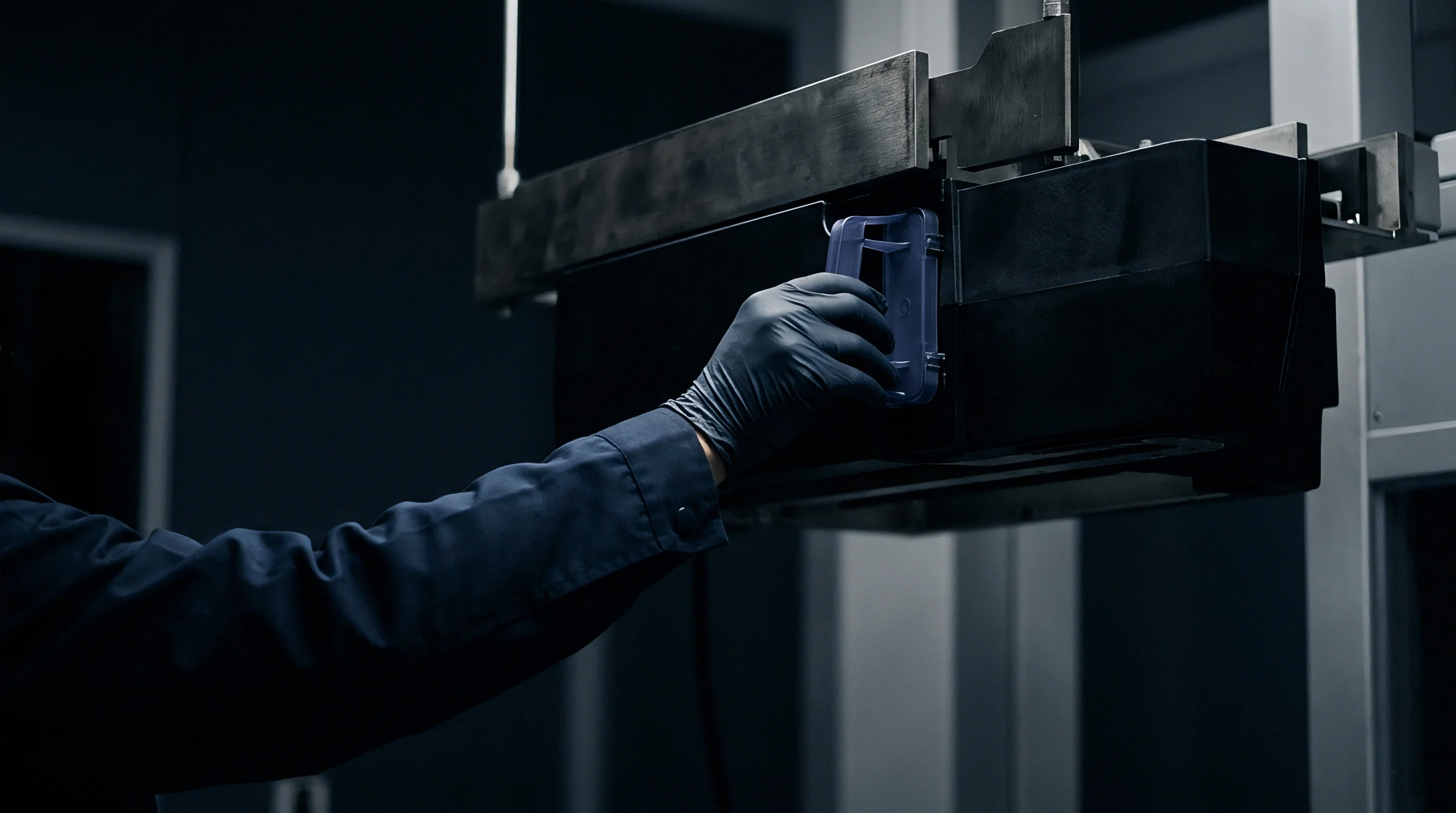
Reinforcing thin copper electroforms transforms delicate shells into rigid insert structures capable of enduring high injection pressures. Electroformed copper shells are typically deposited to a thickness ranging between 1.0 and 3.0 millimeters due to economic constraints associated with long bath residence times. A 2-millimeter pure copper shell lacks the structural rigidity needed to withstand peak cavity pressures of 600 to 1400 bar during injection packing phases, requiring solid structural reinforcement on its non-forming rear face.
Cast Epoxy and Metallic Composite Backings
Aluminum-filled epoxy resins offer an economical backing approach for prototype and short-run production tooling. Epoxies heavily loaded with spherical aluminum powder (80% to 85% mass fraction) exhibit compressive strength between 120 MPa and 160 MPa with a thermal conductivity of 1.5 to 2.5 W/mK. Casting occurs under vacuum (-0.95 bar) to eliminate air pockets that cause localized thermal hot spots or structural crushing during press operation.
Steel backings support high loads. For high-volume production, composite epoxy backings prove inadequate due to low compressive modulus and thermal degradation under continuous 140°C mold operating temperatures. Low-melting-point metallic alloys (such as eutectic copper-tin or zinc-aluminum alloys) cast behind the electroformed shell deliver compressive yields exceeding 400 MPa while maintaining thermal conductivity values above 50 W/mK.
Pure copper electroformed shells backed with aluminum-filled epoxy withstand injection clamping forces up to 800 bar cavity pressure without yield failure.
Co-Deposited Heavy Nickel and Machined Steel Shells
Direct co-deposition of structural nickel over the copper electroform provides high structural integrity for demanding injection applications. Once the initial 1.5-millimeter copper shell deposits inside the sulfamate bath, the insert transfers to a nickel sulfamate bath to deposit a 5-to-10-millimeter structural layer of high-hardness nickel (350 to 450 HV). This nickel-copper bi-metallic construction matches mechanical strength requirements directly behind the molding interface, eliminating mechanical compliance issues inherent to cast composite materials.
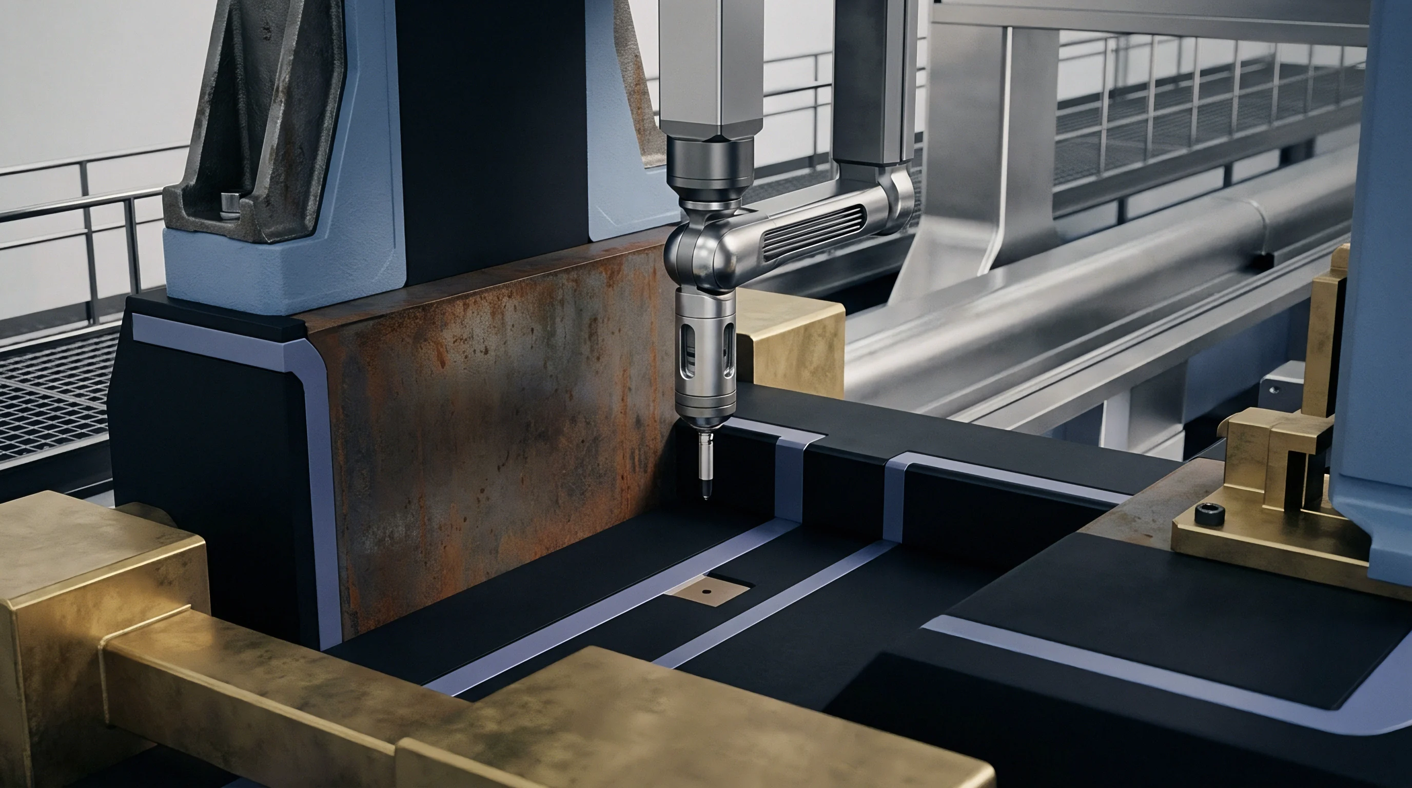
Precision CNC milling and surface grinding shape the rear nickel layer into a square, planar reference mounting surface. Wire electrical discharge machining cuts outer parting line edges relative to micro-features on the front copper face, holding perimeter insert positioning within ±0.005 millimeters inside the main tool steel cavity pocket.
- Compressive Load Calculation compares peak cavity pressure against composite material yield strength to prevent permanent insert deformation under packing loads.
- Thermal Expansion Matching aligns the thermal expansion coefficient of the support material with pure electroformed copper to prevent thermal fatigue cracking.
- Parting Line Machining Allowance reserves minimum 1.5 millimeter stock thickness for precision wire electrical discharge machining of outer mounting interfaces.
- Cooling Channel Integration embeds copper tubing directly into cast backings to optimize heat extraction rates during molding cycles.
Selecting backing materials with mismatched thermal expansion coefficients relative to pure copper generates cyclical shear stresses at the interface during press warm-up, eventually causing bond delamination and insert failure.
Injection
Thermal performance in press-side molding operations relies on the elevated thermal conductivity of pure copper cavity walls. Pure electroformed copper demonstrates a thermal conductivity of approximately 390 W/mK, dwarfing standard tool steel grades such as 1.2344 (H13) which hover near 24 W/mK. High thermal conductivity rapidly transfers heat away from molten polymer, reducing cooling phase times while maintaining tight dimensional tolerances on molded plastic parts.

Thermal Conductivity and Cycle Time Reduction
Cooling cycle duration controls production economics in thin-wall plastics injection. Pure copper dissipates thermal energy rapidly. Heat conducts away from the plastic melt up to fifteen times faster through a copper insert than through standard tool steel cavity walls.
In a representative packaging application molding polypropylene (PP) with a 1.2-millimeter wall section, replacing H13 steel inserts with 2-millimeter electroformed copper inserts reduces overall cycle time from 8.5 seconds down to 5.2 seconds, representing a 38.8% output increase on the same press platform.
Rapid thermal evacuation flattens internal temperature gradients across thick-to-thin part section transitions. Uniform cooling rates suppress differential volumetric shrinkage, which eliminates sink marks on cosmetic surfaces and prevents part warpage without requiring excessive packing pressure profiles.
High thermal diffusivity of copper inserts shortens cooling phase duration while demanding precise mold temperature control to prevent freeze-off at the gate.
| Insert Material Construction | Thermal Conductivity (W/mK) | Cooling Phase Duration (s) | Core Surface Temp Drift (°C) | Maximum Service Life (Shots) |
|---|---|---|---|---|
| Standard H13 Tool Steel | 24.3 | 6.8 | ±8.5 | 1,000,000 |
| Electroformed Cu + Epoxy Backing | 385.0 (Shell) / 2.1 (Backing) | 4.9 | ±12.0 | 100,000 |
| Electroformed Cu + Cast Zn-Al Backing | 385.0 (Shell) / 95.0 (Backing) | 3.8 | ±3.2 | 500,000 |
| Co-Deposited Cu-Ni Bi-Metal Shell | 385.0 (Cu) / 90.0 (Ni) | 4.1 | ±2.5 | 750,000 |
Where Do Micro-Feature Tolerances Shift during High-Volume Runs?
Continuous thermal cycling and abrasive polymer flow wear micro-textured details on electroformed copper faces over extended production runs. Pure copper exhibits relatively low scratch resistance and surface hardness (typically 100 to 140 HV in unalloyed deposits), rendering fine sub-micron optical textures vulnerable to erosion when processing glass-filled resins like PA66-GF30 or abrasive filled polymers. Micro-feature peak heights degrade gradually, shifting light diffraction angles or fluid wetting behavior on molded parts after 50,000 press cycles.
Thin physical vapor deposition coatings apply protective barriers over copper micro-structures without rounding sharp detail edges. A 1.5-micrometer layer of titanium nitride (TiN) or diamond-like carbon (DLC) applied at temperatures below 150°C increases surface hardness beyond 2200 HV. Hardened coatings extend cavity operational life past 500,000 shots while preserving sub-micron feature fidelity under high melt shear stress conditions.
Whether nano-scale feature fatigue originates from localized thermal expansion mismatches between the PVD hard coating and the soft copper substrate remains an open question under long-term industrial production conditions.
Sourcing
Procuring electroformed tooling requires evaluating master-making overhead against cavity volume targets and piece-price economics. Electroforming eliminates expensive 5-axis CNC micro-milling operations for multi-cavity tooling by using a single reusable master mandrel to replicate identical copper inserts. This replication capability shifts tooling investment from individual cavity machining costs toward initial master pattern creation.
Cavitation Cost Amortization and Tooling Economics
Master mandrel creation accounts for up to 60% of total initial tooling expenditures when producing complex micro-structured inserts. Once an optical-grade silicon master or micro-machined brass mandrel passes dimensional audit, electroforming additional identical inserts scales at linear chemical deposition costs. For high-cavitation production molds (such as 32-cavity or 64-cavity optical lens tools), electroforming lowers total tool procurement expenses compared to direct diamond-turning each individual steel cavity block.
A worked financial scenario demonstrates this amortization shift across a 16-cavity micro-fluidic part program. Direct ultra-precision micro-milling of 16 individual tool steel inserts costs 144,000 USD (8,000 USD per cavity) with a cumulative dimensional tolerance band of ±8.0 micrometers across the cavity set. Fabrication of one high-precision silicon master mandrel costs 25,000 USD, while electroforming 16 copper inserts from that master costs 2,500 USD per insert shell plus 1,500 USD per backing block.
Total electroformed tooling procurement drops to 89,000 USD—delivering a 38.1% upfront capital cost savings while tightening inter-cavity dimensional variation within a ±1.5 micrometer band.
Quality Acceptance Specifications and Verification Protocols
Procurement documents for electroformed inserts demand strict acceptance metrics covering physical shell integrity, backing bond quality, and 3D surface geometry. Non-destructive testing via ultrasonic immersion scanning verifies the absence of internal voids, delamination zones, or air inclusions within cast backing interfaces before final toolroom assembly. Dimensional inspection mandates optical white-light interferometry or confocal microscopy to measure micro-feature profile fidelity against master CAD geometry prior to mold trial sign-off.
Tooling sign-off agreements specify First Article Inspection (FAI) reports containing 3D surface roughness parameters (Sa and Sz defined per ISO 25178) measured at nine designated evaluation points across the active insert surface. Inserts exhibiting localized thickness variations exceeding 20 micrometers or internal micro-void density greater than 0.05 per square millimeter face immediate lot rejection. Establishing these technical criteria upfront protects sourcing budgets, securing high-precision tooling performance across long-term manufacturing operations.