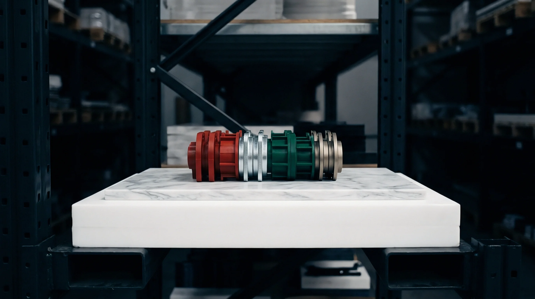
Electroformed Copper Inserts for Millimeter-Wave Tool Steel Tooling Assemblies
Electroformed copper inserts enable sub-30nm surface roughness and 35% faster cycle times in mmWave tooling when thermal expansion gaps are engineered.
Electrical energy dissipation occurring within metallic circuit pathways on electronic substrates stems from finite material conductivity and alternating current resistance. In moulded interconnect devices and high-frequency polymer assemblies, conductor loss defines the attenuation of radio frequency signals as energy dissipates into heat along plated copper traces. At gigahertz operational frequencies, current restricts itself to the thin outer skin layer of the conductor, magnifying the impact of metal surface roughness.
Polymer substrates must provide smooth surface finishes and stable anchor profiles so electroplated layers retain minimal resistance while maintaining mechanical peel strength. The boundary of this mechanism applies strictly to ohmic dissipation within the metallized trace itself, distinct from dielectric absorption occurring in the adjacent polymer substrate.
Chemical metallization of three-dimensional injection moulded substrates relies on surface etching or laser direct structuring to anchor copper layers onto the plastic core. Increased surface roughness promotes strong mechanical adhesion between the plated metal and the polymer, but excessive surface peaks dramatically increase conductor loss at high signal frequencies. Current flowing within the limited skin depth must travel over microscopic metal contours, lengthening the effective physical path and increasing electrical resistance.
Tool surface polishing directly governs the initial moulded plastic topography, influencing how smooth the subsequent seed layer can be. Moulding engineers adjust cavity polish to balance trace adhesion requirements against high-frequency transmission loss constraints. Regrind resin contamination alters chemical etching rates, creating erratic surface profiles that degrade electrical performance across production lots.
Dimensional stability of the underlying resin prevents trace cracking and micro-fractures under operational thermal cycling. Polyphthalamides and liquid crystal polymers provide high deflection temperatures and low moisture absorption, stabilizing the trace geometry under power dissipation. When conductor loss heats the metallic trace during operation, the difference in thermal expansion between the metal and the polymer creates interface shear stresses.
Delamination occurs if interfacial bond strength degrades under this localized ohmic heating. Material datasheets specify thermal conductivity values that indicate how effectively the substrate can carry dissipated heat away from the circuit traces. Toolmakers maintain uniform part wall thicknesses to prevent localized warping that could distort trace alignment or induce mechanical strain in the metal layer.
Fabricating electronic pathways on moulded substrates requires tight control over electroplating thickness and chemical bath composition. Insufficient copper deposition leaves thin metal cross-sections that accelerate resistive heating, while uneven current density creates thickness variations across three-dimensional part contours. Quality control involves measuring surface profile roughness with optical profilometers and verifying trace resistance using four-point probe stations.
Plating defects, such as nodule formation or chemical pitting, trigger scrap by locally spiking signal attenuation. Moulders monitor hold pressure and melt temperature closely, because poor molecular orientation creates internal stresses that cause plating blisters during post-moulding thermal cures. Trace integrity verification ensures final electronic assemblies satisfy functional radio frequency attenuation specifications under sustained operating loads.
Electroformed copper inserts enable sub-30nm surface roughness and 35% faster cycle times in mmWave tooling when thermal expansion gaps are engineered.
Expertise is a utility, not a secret. sentiention™ publishes its working knowledge as open reference: intelligence layer covering the materials it sources, the markets it enters, and the reference that serves both.